Understanding Digital Logic Design
Extra materials for the combined MIPSfpga and Connected MCU seminar by Imagination Technologies
October-November 2016
Quiz 2.1 - Combinational Logic
Name ___________________________________________________________________
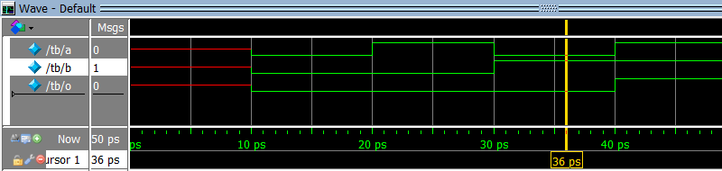
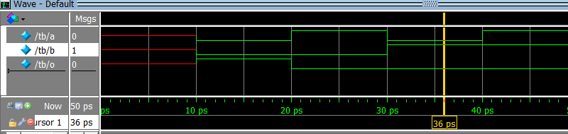
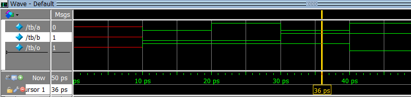
1. Which waveform is the result of the simulation below?
module design (input a, input b, output o);
assign o = ~ a | ~ b;
endmodule
module tb;
logic a, b, o;
design design_inst (a, b, o);
initial
begin
$dumpvars;
$monitor ("%t a %b b %b o %b", $time, a, b, o);
#10;
a = 0; b = 0; #10;
a = 1; b = 0; #10;
a = 0; b = 1; #10;
a = 1; b = 1; #10;
end
endmodule
a)
 b)
b)
 c)
c)
 d)
d)
 e)
e)
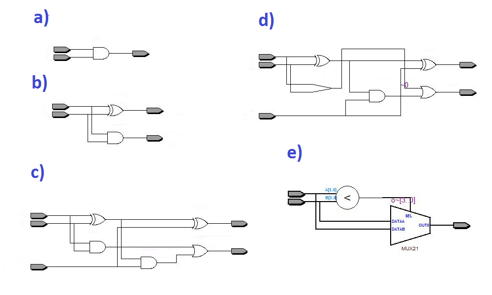
 2. What is the result of synthesis of this module?
module design
(
input a,
input b,
output sum,
output carry
);
assign sum = a ^ b;
assign carry = a & b;
endmodule
2. What is the result of synthesis of this module?
module design
(
input a,
input b,
output sum,
output carry
);
assign sum = a ^ b;
assign carry = a & b;
endmodule
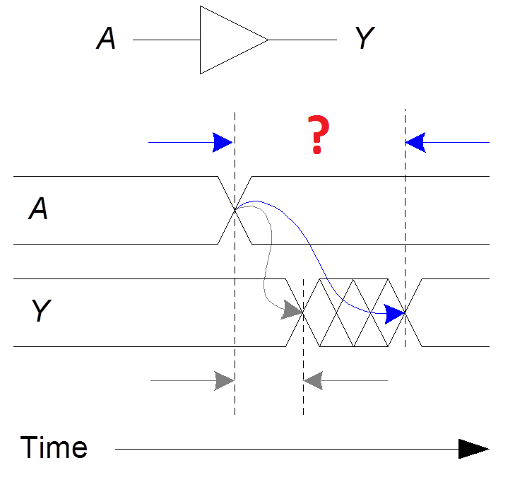
 3. What kind of delay is illustrated on the picture below (marked by "?")?
a) Propagation delay: tpd = max delay from input to output
b) Contamination delay: tcd = min delay from input to output
3. What kind of delay is illustrated on the picture below (marked by "?")?
a) Propagation delay: tpd = max delay from input to output
b) Contamination delay: tcd = min delay from input to output
 Sources of some pictures:
Slides from Steve Harris and Sarah Harris that accompany textbook
Digital Design and Computer Architecture, Second Edition by David Harris and Sarah Harris, 2012
Quiz is created by Yuri Panchul
Sources of some pictures:
Slides from Steve Harris and Sarah Harris that accompany textbook
Digital Design and Computer Architecture, Second Edition by David Harris and Sarah Harris, 2012
Quiz is created by Yuri Panchul