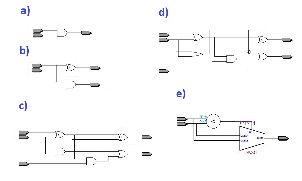
 b)
b)
 c)
c)
 d)
d)
 e)
e)
 2. What is the result of synthesis of this module?
module design
(
input [3:0] a,
input [3:0] b,
output [3:0] o
);
assign o = a < b ? a : b;
endmodule
2. What is the result of synthesis of this module?
module design
(
input [3:0] a,
input [3:0] b,
output [3:0] o
);
assign o = a < b ? a : b;
endmodule
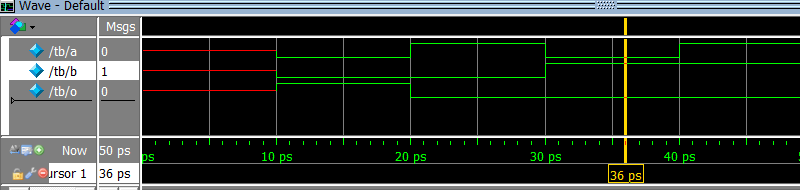
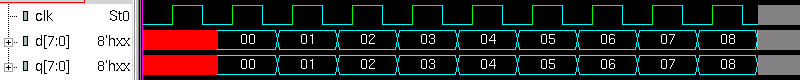
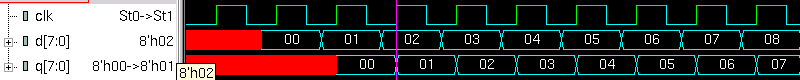
 3. Which waveform is the simulation result of Verilog code below?
module dut
(
input clk,
input [7:0] d,
output logic [7:0] q
);
logic [7:0] r;
always @(posedge clk)
begin
r = d;
q <= r;
end
endmodule
module testbench;
logic clk;
logic [7:0] d, q;
dut dut (clk, d, q);
initial
begin
clk = 0;
forever
end
initial
begin
$dumpvars ();
for (int i = 0; i < 10; i++)
begin
@(posedge clk);
d = i;
end
$finish;
end
endmodule
a)
3. Which waveform is the simulation result of Verilog code below?
module dut
(
input clk,
input [7:0] d,
output logic [7:0] q
);
logic [7:0] r;
always @(posedge clk)
begin
r = d;
q <= r;
end
endmodule
module testbench;
logic clk;
logic [7:0] d, q;
dut dut (clk, d, q);
initial
begin
clk = 0;
forever
end
initial
begin
$dumpvars ();
for (int i = 0; i < 10; i++)
begin
@(posedge clk);
d = i;
end
$finish;
end
endmodule
a)
 b)
b)
 c)
c)
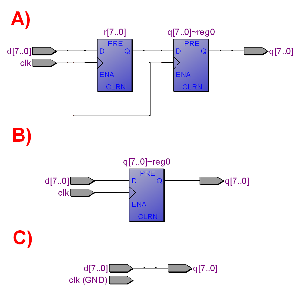
 4. What schematics correspond to Verilog code below?
module dut
(
input clk,
input [7:0] d,
output logic [7:0] q
);
logic [7:0] r;
always @(posedge clk)
begin
r = d;
q <= r;
end
endmodule
4. What schematics correspond to Verilog code below?
module dut
(
input clk,
input [7:0] d,
output logic [7:0] q
);
logic [7:0] r;
always @(posedge clk)
begin
r = d;
q <= r;
end
endmodule
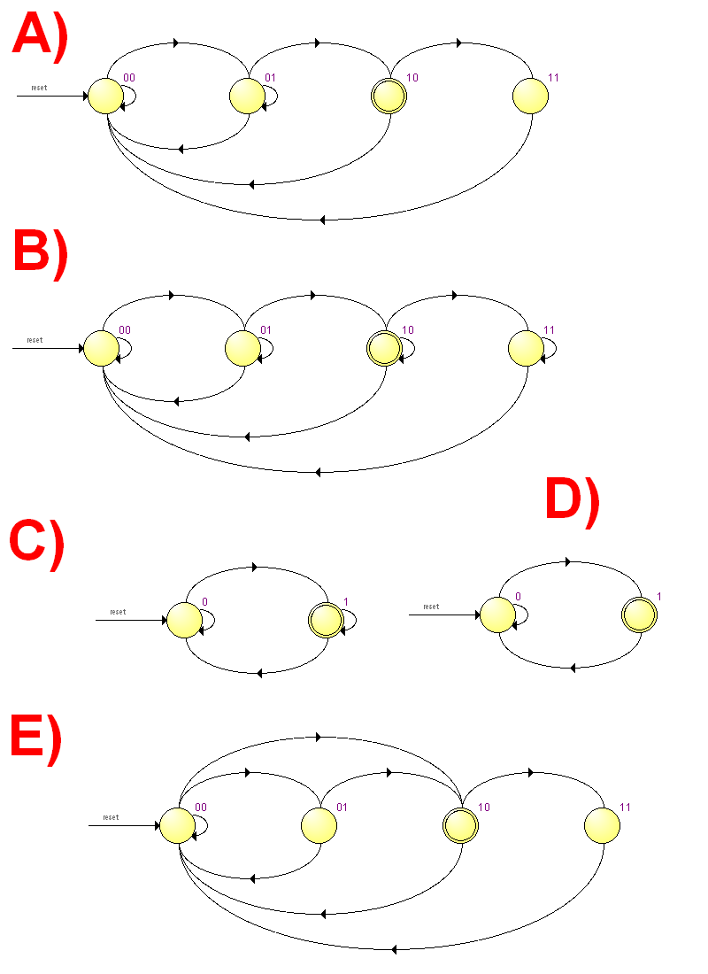
 5. What Finite State Machine (FSM) state diagram correspond to Verilog code below?
module dut
(
input clk,
input resetn,
input a,
output b
);
logic [0:0] state;
always @(posedge clk)
if (! resetn)
state <= 0;
else
case (state)
0: state <= 1;
1: state <= 0;
endcase
assign b = (state == 1);
endmodule
5. What Finite State Machine (FSM) state diagram correspond to Verilog code below?
module dut
(
input clk,
input resetn,
input a,
output b
);
logic [0:0] state;
always @(posedge clk)
if (! resetn)
state <= 0;
else
case (state)
0: state <= 1;
1: state <= 0;
endcase
assign b = (state == 1);
endmodule
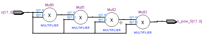
The code below contains three modules implementing the same functionality, calculating the power of five of a given number. Analyze the code and answer the following questions: module pow_5_implementation_1 ( input clock, input reset_n, input run, input [17:0] n, output ready, output [17:0] n_pow_5 ); reg [4:0] shift; always @(posedge clock or negedge reset_n) if (! reset_n) shift <= 0; else if (run) shift <= 5'b10000; else shift <= shift >> 1; assign ready = shift [0]; reg [17:0] r_n, mul; always @(posedge clock) if (run) begin r_n <= n; mul <= n; end else begin mul <= mul * r_n; end assign n_pow_5 = mul; endmodule //-------------------------------------------------------------------- module pow_5_implementation_2 ( input clock, input [17:0] n, output reg [17:0] n_pow_5 ); reg [17:0] n_1, n_2, n_3; reg [17:0] n_pow_2, n_pow_3, n_pow_4; always @(posedge clock) begin n_1 <= n; n_2 <= n_1; n_3 <= n_2; n_pow_2 <= n * n; n_pow_3 <= n_pow_2 * n_1; n_pow_4 <= n_pow_3 * n_2; n_pow_5 <= n_pow_4 * n_3; end endmodule //-------------------------------------------------------------------- module pow_5_implementation_3 ( input [17:0] n, output [17:0] n_pow_5 ); assign n_pow_5 = n * n * n * n * n; endmodule
6. Which implementation is purely combinational? a) pow_5_implementation_1 b) pow_5_implementation_2 c) pow_5_implementation_3 d) pow_5_implementation_1 and pow_5_implementation_2 e) pow_5_implementation_1 and pow_5_implementation_3 f) pow_5_implementation_2 and pow_5_implementation_3 g) all of them h) none of them
7. Which implementation is sequential? a) pow_5_implementation_1 b) pow_5_implementation_2 c) pow_5_implementation_3 d) pow_5_implementation_1 and pow_5_implementation_2 e) pow_5_implementation_1 and pow_5_implementation_3 f) pow_5_implementation_2 and pow_5_implementation_3 g) all of them h) none of them
8. Which implementation is pipelined? a) pow_5_implementation_1 b) pow_5_implementation_2 c) pow_5_implementation_3 d) pow_5_implementation_1 and pow_5_implementation_2 e) pow_5_implementation_1 and pow_5_implementation_3 f) pow_5_implementation_2 and pow_5_implementation_3 g) all of them h) none of them
9. Identify the implementation that corresponds to the following schematics: a) pow_5_implementation_1 b) pow_5_implementation_2 c) pow_5_implementation_3 d) pow_5_implementation_1 and pow_5_implementation_2 e) pow_5_implementation_1 and pow_5_implementation_3 f) pow_5_implementation_2 and pow_5_implementation_3 g) all of them h) none of them
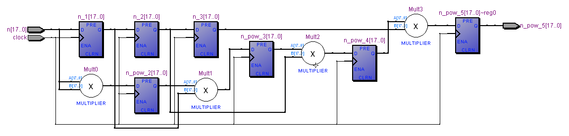
10. Identify the implementation that corresponds to the following schematics: a) pow_5_implementation_1 b) pow_5_implementation_2 c) pow_5_implementation_3 d) pow_5_implementation_1 and pow_5_implementation_2 e) pow_5_implementation_1 and pow_5_implementation_3 f) pow_5_implementation_2 and pow_5_implementation_3 g) all of them h) none of them
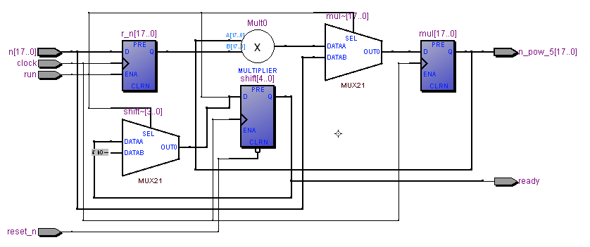
11. Identify the implementation that corresponds to the following schematics: a) pow_5_implementation_1 b) pow_5_implementation_2 c) pow_5_implementation_3 d) pow_5_implementation_1 and pow_5_implementation_2 e) pow_5_implementation_1 and pow_5_implementation_3 f) pow_5_implementation_2 and pow_5_implementation_3 g) all of them h) none of them
12. Which implementation is likely to allow the highest maximum frequency (assuming that the outputs of the combinational implementation are connected to clocked register)? a) pow_5_implementation_1 b) pow_5_implementation_2 c) pow_5_implementation_3
13. Which implementation is likely to use the smallest number of gates? a) pow_5_implementation_1 b) pow_5_implementation_2 c) pow_5_implementation_3
14. Which implementation is likely to have the highest throughput (number of calculated pow_5(n) results per seconds)? a) pow_5_implementation_1 b) pow_5_implementation_2 c) pow_5_implementation_3
15. Which implementation is going to have the smallest latency in clock cycles (assuming that the outputs of the combinational implementation are connected to clocked registers)? a) pow_5_implementation_1 b) pow_5_implementation_2 c) pow_5_implementation_3
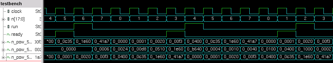
16. The testbench instantiated all three implementations of pow_5. module testbench; reg clock; reg reset_n; reg run; reg [17:0] n; wire ready; wire [17:0] n_pow_5_implementation_1; wire [17:0] n_pow_5_implementation_2; wire [17:0] n_pow_5_implementation_3; initial begin clock = 1; forever # 50 clock = ! clock; end initial begin repeat (2) @(posedge clock); reset_n <= 0; repeat (2) @(posedge clock); reset_n <= 1; end pow_5_implementation_1 pow_5_implementation_1 (clock, reset_n, run, n, ready, n_pow_5_implementation_1); pow_5_implementation_2 pow_5_implementation_2 (clock, n, n_pow_5_implementation_2); pow_5_implementation_3 pow_5_implementation_3 (n, n_pow_5_implementation_3); integer i; initial begin $dumpvars; $monitor ("clock %b reset_n %b n %d comb %d seq %d run %b ready %b pipe %d", clock, reset_n, n, n_pow_5_implementation_1, n_pow_5_implementation_2, run, ready, n_pow_5_implementation_3); @(posedge reset_n); @(posedge clock); for (i = 0; i < 50; i = i + 1) begin n <= i & 7; run <= (i == 0 || ready); @(posedge clock); end $finish; end endmodule
An engineer simulated the testbench and got the following waveform. However he forgot the order he added the last three signals to the waveform. Can you determine which signal is the output of combinational implementation, sequential non-pipelined implementation and sequential pipelined implementation? a) The order is (from upper n_pow_5... to lower n_pow_5...): combinational, sequential non-pipelined implementation, pipelined b) combinational, pipelined, sequential non-pipelined implementation c) pipelined, combinational, sequential non-pipelined implementation d) pipelined, sequential non-pipelined implementation, combinational e) sequential non-pipelined implementation, combinational, pipelined f) sequential non-pipelined implementation, pipelined, combinational
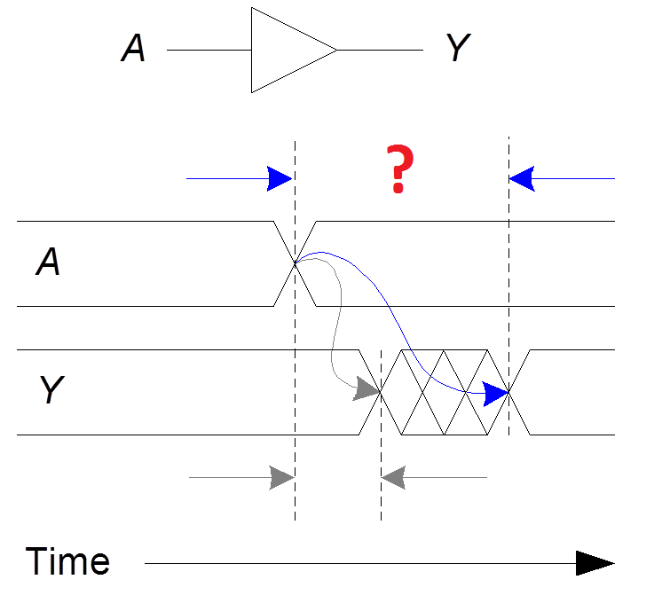
 17. What kind of delay is illustrated on the picture below (marked by "?")?
a) Propagation delay: tpd = max delay from input to output
b) Contamination delay: tcd = min delay from input to output
c) Skew: difference between two clock edges. The clock doesn�t arrive at all registers at same time.
17. What kind of delay is illustrated on the picture below (marked by "?")?
a) Propagation delay: tpd = max delay from input to output
b) Contamination delay: tcd = min delay from input to output
c) Skew: difference between two clock edges. The clock doesn�t arrive at all registers at same time.
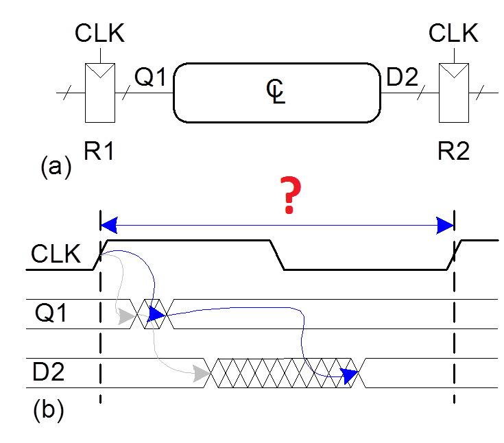
 18. What kind of timing constraint is illustrated on the picture below (marked by "?")?
a) Setup time: tsetup = time before clock edge data must be stable (i.e. not changing)
b) Hold time: thold = time after clock edge data must be stable
c) Aperture time: ta = time around clock edge data must be stable (ta = tsetup + thold)
d) Tc = minimum and maximum delays between registers
18. What kind of timing constraint is illustrated on the picture below (marked by "?")?
a) Setup time: tsetup = time before clock edge data must be stable (i.e. not changing)
b) Hold time: thold = time after clock edge data must be stable
c) Aperture time: ta = time around clock edge data must be stable (ta = tsetup + thold)
d) Tc = minimum and maximum delays between registers
 19. Which rule for signal assignment is violated in the following code?
a) Synchronous sequential logic: use always @(posedge clk) or always_ff @(posedge clk)
and nonblocking assignments (<=)
always_ff @ (posedge clk)
q <= d; // nonblocking
b) Simple combinational logic: use continuous assignments (assign�)
assign y = a & b;
c) More complicated combinational logic: use always @* or always_comb and blocking assignments (=)
d) Assign a signal in only one always statement or continuous assignment statement
e) This code does not violate any rules for signal assignment
module dut
(
input clk,
input [7:0] d,
output logic [7:0] q
);
always @(posedge clk)
if (d == 3)
q <= 4;
always @(posedge clk)
if (d == 7)
q <= 1;
endmodule
20. Write the missing code near red comments
// Combinational building block: multiplexor
module mux_2_1
(
input [3:0] d0,
input [3:0] d1,
input sel,
output [3:0] y
);
assign y = sel ? d1 : d0;
endmodule
module mux_4_1_imp_1
(
input [3:0] d0, d1, d2, d3,
input [1:0] sel,
output [3:0] y
);
assign y = sel [1]
? (sel [0] ? d3 : d2)
: (sel [0] ? d1 : d0);
endmodule
module mux_4_1_imp_2
(
input [3:0] d0, d1, d2, d3,
input [1:0] sel,
output reg [3:0] y
);
// Using code for mux_4_1_imp_1 as a reference,
// write code for 4:1 mux using "case" statement
endmodule
module mux_4_1_imp_3
(
input [3:0] d0, d1, d2, d3,
input [1:0] sel,
output [3:0] y
);
// Construct 4:1 mux using three instances of mux_2_1 modules
endmodule
module mux_4_1_bits_2
(
input [1:0] d0, d1, d2, d3,
input [1:0] sel,
output [1:0] y
);
assign y = sel [1]
? (sel [0] ? d3 : d2)
: (sel [0] ? d1 : d0);
endmodule
module mux_4_1_imp_4
(
input [3:0] d0, d1, d2, d3,
input [1:0] sel,
output [3:0] y
);
// Construct 4:1 mux with 4-bit inputs and output
// using two instances of mux_4_1 modules with 2-bit inputs and outputs
//
//
//
//
//
//
//
//
//
//
//
//
//
//
//
//
//
//
//
endmodule
module basys3_2
(
input clk,
input btnC,
input btnU,
input btnL,
input btnR,
input btnD,
input [15:0] sw,
output [15:0] led,
output [ 6:0] seg,
output dp,
output [ 3:0] an
);
mux_4_1_imp_1
(
// Write code that connects module's inputs and output:
// d0 - to sw [ 3: 0]
// d1 - to sw [ 7: 4]
// d2 - to sw [11: 8]
// d3 - to sw [15:12]
// sel [1] - to btnC
// sel [0] - to btnR
// y - to led [ 3: 0]
);
assign seg = ~ 7'b0;
assign dp = 1'b1;
assign an = 4'b0;
endmodule
//--------------------------------------------------------------------
// Combinational building block: decoder
module decoder_3_8_imp_1
(
input [2:0] a,
output reg [7:0] y
);
always @*
case (a)
3'b000: y = 8'b00000001;
3'b001: y = 8'b00000010;
3'b010: y = 8'b00000100;
3'b011: y = 8'b00001000;
3'b100: y = 8'b00010000;
3'b101: y = 8'b00100000;
3'b110: y = 8'b01000000;
3'b111: y = 8'b10000000;
endcase
endmodule
module decoder_3_8_imp_2
(
input [2:0] a,
output reg [7:0] y
);
always @*
begin
y = 0;
y [a] = 1;
end
endmodule
module decoder_3_8_imp_3
(
input [2:0] a,
output [7:0] y
);
// Using decoder_3_8_imp_1 and decoder_3_8_imp_2 as references,
// implement the decoder using shift operation
//
//
endmodule
module basys3_3
(
input clk,
input btnC,
input btnU,
input btnL,
input btnR,
input btnD,
input [15:0] sw,
output [15:0] led,
output [ 6:0] seg,
output dp,
output [ 3:0] an
);
decoder_3_8_imp_1 decoder_3_8_imp_1 (.a (sw [3:0]), .y (led [ 7:0]));
decoder_3_8_imp_2 decoder_3_8_imp_3 (.a (sw [3:0]), .y (led [15:8]));
assign seg = ~ 7'b0;
assign dp = 1'b1;
assign an = 4'b0;
endmodule
//--------------------------------------------------------------------
// Combinational building block: seven-segment driver
module single_digit_display
(
input [3:0] digit,
input single_digit,
input show_dot,
output reg [6:0] seven_segments,
output dot,
output [3:0] anodes
);
always @*
case (digit)
'h0: seven_segments = 'b1000000; // a b c d e f g
'h1: seven_segments = 'b1111001;
'h2: seven_segments = 'b0100100; // --a--
'h3: seven_segments = 'b0110000; // | |
'h4: seven_segments = 'b0011001; // f b
'h5: seven_segments = 'b0010010; // | |
'h6: seven_segments = 'b0000010; // --g--
'h7: seven_segments = 'b1111000; // | |
'h8: seven_segments = 'b0000000; // e c
'h9: seven_segments = 'b0011000; // | |
'ha: seven_segments = 'b0001000; // --d--
'hb: seven_segments = 'b0000011;
'hc: seven_segments = 'b1000110;
'hd: /* Fill the missing code */;
'he: seven_segments = 'b0000110;
'hf: seven_segments = 'b0001110;
endcase
assign dot = ~ show_dot;
assign anodes = single_digit ? 4'b1110 : 4'b0000;
endmodule
//--------------------------------------------------------------------
module basys3_5
(
input clk,
input btnC,
input btnU,
input btnL,
input btnR,
input btnD,
input [15:0] sw,
output [15:0] led,
output [ 6:0] seg,
output dp,
output [ 3:0] an
);
single_digit_display single_digit_display
(
.digit ( sw [3:0] ),
.single_digit ( sw [15] ),
.show_dot ( sw [14] ),
.seven_segments ( seg ),
.dot ( dp ),
.anodes ( an )
);
endmodule
//--------------------------------------------------------------------
// Sequential building block: counter
module clock_divider_100_MHz_to_1_49_Hz
(
input clock_100_MHz,
input resetn,
output clock_1_49_Hz
);
// 100 MHz / 2 ** 26 = 1.49 Hz
reg [25:0] counter;
always /* Fill the missing code */
begin
if (! resetn)
counter <= 0;
else
counter <= counter + 1;
end
// Write code connecting bit 25 of the counter to the output
endmodule
module counter
(
input clock,
input resetn,
output reg [15:0] count
);
always @ (posedge clock or negedge resetn)
begin
if (! resetn)
count <= 0;
else
count <= count + 1;
end
endmodule
module basys3_6
(
input clk,
input btnC,
input btnU,
input btnL,
input btnR,
input btnD,
input [15:0] sw,
output [15:0] led,
output [ 6:0] seg,
output dp,
output [ 3:0] an
);
wire clock;
wire resetn = ! btnU;
clock_divider_100_MHz_to_1_49_Hz clock_divider
(
.clock_100_MHz (clk),
.resetn (resetn),
.clock_1_49_Hz (clock)
);
counter counter
(
.clock ( clock ),
.resetn ( resetn ),
.count ( led )
);
assign seg = ~ 7'b0;
assign dp = 1'b0;
assign an = 4'b0;
endmodule
19. Which rule for signal assignment is violated in the following code?
a) Synchronous sequential logic: use always @(posedge clk) or always_ff @(posedge clk)
and nonblocking assignments (<=)
always_ff @ (posedge clk)
q <= d; // nonblocking
b) Simple combinational logic: use continuous assignments (assign�)
assign y = a & b;
c) More complicated combinational logic: use always @* or always_comb and blocking assignments (=)
d) Assign a signal in only one always statement or continuous assignment statement
e) This code does not violate any rules for signal assignment
module dut
(
input clk,
input [7:0] d,
output logic [7:0] q
);
always @(posedge clk)
if (d == 3)
q <= 4;
always @(posedge clk)
if (d == 7)
q <= 1;
endmodule
20. Write the missing code near red comments
// Combinational building block: multiplexor
module mux_2_1
(
input [3:0] d0,
input [3:0] d1,
input sel,
output [3:0] y
);
assign y = sel ? d1 : d0;
endmodule
module mux_4_1_imp_1
(
input [3:0] d0, d1, d2, d3,
input [1:0] sel,
output [3:0] y
);
assign y = sel [1]
? (sel [0] ? d3 : d2)
: (sel [0] ? d1 : d0);
endmodule
module mux_4_1_imp_2
(
input [3:0] d0, d1, d2, d3,
input [1:0] sel,
output reg [3:0] y
);
// Using code for mux_4_1_imp_1 as a reference,
// write code for 4:1 mux using "case" statement
endmodule
module mux_4_1_imp_3
(
input [3:0] d0, d1, d2, d3,
input [1:0] sel,
output [3:0] y
);
// Construct 4:1 mux using three instances of mux_2_1 modules
endmodule
module mux_4_1_bits_2
(
input [1:0] d0, d1, d2, d3,
input [1:0] sel,
output [1:0] y
);
assign y = sel [1]
? (sel [0] ? d3 : d2)
: (sel [0] ? d1 : d0);
endmodule
module mux_4_1_imp_4
(
input [3:0] d0, d1, d2, d3,
input [1:0] sel,
output [3:0] y
);
// Construct 4:1 mux with 4-bit inputs and output
// using two instances of mux_4_1 modules with 2-bit inputs and outputs
//
//
//
//
//
//
//
//
//
//
//
//
//
//
//
//
//
//
//
endmodule
module basys3_2
(
input clk,
input btnC,
input btnU,
input btnL,
input btnR,
input btnD,
input [15:0] sw,
output [15:0] led,
output [ 6:0] seg,
output dp,
output [ 3:0] an
);
mux_4_1_imp_1
(
// Write code that connects module's inputs and output:
// d0 - to sw [ 3: 0]
// d1 - to sw [ 7: 4]
// d2 - to sw [11: 8]
// d3 - to sw [15:12]
// sel [1] - to btnC
// sel [0] - to btnR
// y - to led [ 3: 0]
);
assign seg = ~ 7'b0;
assign dp = 1'b1;
assign an = 4'b0;
endmodule
//--------------------------------------------------------------------
// Combinational building block: decoder
module decoder_3_8_imp_1
(
input [2:0] a,
output reg [7:0] y
);
always @*
case (a)
3'b000: y = 8'b00000001;
3'b001: y = 8'b00000010;
3'b010: y = 8'b00000100;
3'b011: y = 8'b00001000;
3'b100: y = 8'b00010000;
3'b101: y = 8'b00100000;
3'b110: y = 8'b01000000;
3'b111: y = 8'b10000000;
endcase
endmodule
module decoder_3_8_imp_2
(
input [2:0] a,
output reg [7:0] y
);
always @*
begin
y = 0;
y [a] = 1;
end
endmodule
module decoder_3_8_imp_3
(
input [2:0] a,
output [7:0] y
);
// Using decoder_3_8_imp_1 and decoder_3_8_imp_2 as references,
// implement the decoder using shift operation
//
//
endmodule
module basys3_3
(
input clk,
input btnC,
input btnU,
input btnL,
input btnR,
input btnD,
input [15:0] sw,
output [15:0] led,
output [ 6:0] seg,
output dp,
output [ 3:0] an
);
decoder_3_8_imp_1 decoder_3_8_imp_1 (.a (sw [3:0]), .y (led [ 7:0]));
decoder_3_8_imp_2 decoder_3_8_imp_3 (.a (sw [3:0]), .y (led [15:8]));
assign seg = ~ 7'b0;
assign dp = 1'b1;
assign an = 4'b0;
endmodule
//--------------------------------------------------------------------
// Combinational building block: seven-segment driver
module single_digit_display
(
input [3:0] digit,
input single_digit,
input show_dot,
output reg [6:0] seven_segments,
output dot,
output [3:0] anodes
);
always @*
case (digit)
'h0: seven_segments = 'b1000000; // a b c d e f g
'h1: seven_segments = 'b1111001;
'h2: seven_segments = 'b0100100; // --a--
'h3: seven_segments = 'b0110000; // | |
'h4: seven_segments = 'b0011001; // f b
'h5: seven_segments = 'b0010010; // | |
'h6: seven_segments = 'b0000010; // --g--
'h7: seven_segments = 'b1111000; // | |
'h8: seven_segments = 'b0000000; // e c
'h9: seven_segments = 'b0011000; // | |
'ha: seven_segments = 'b0001000; // --d--
'hb: seven_segments = 'b0000011;
'hc: seven_segments = 'b1000110;
'hd: /* Fill the missing code */;
'he: seven_segments = 'b0000110;
'hf: seven_segments = 'b0001110;
endcase
assign dot = ~ show_dot;
assign anodes = single_digit ? 4'b1110 : 4'b0000;
endmodule
//--------------------------------------------------------------------
module basys3_5
(
input clk,
input btnC,
input btnU,
input btnL,
input btnR,
input btnD,
input [15:0] sw,
output [15:0] led,
output [ 6:0] seg,
output dp,
output [ 3:0] an
);
single_digit_display single_digit_display
(
.digit ( sw [3:0] ),
.single_digit ( sw [15] ),
.show_dot ( sw [14] ),
.seven_segments ( seg ),
.dot ( dp ),
.anodes ( an )
);
endmodule
//--------------------------------------------------------------------
// Sequential building block: counter
module clock_divider_100_MHz_to_1_49_Hz
(
input clock_100_MHz,
input resetn,
output clock_1_49_Hz
);
// 100 MHz / 2 ** 26 = 1.49 Hz
reg [25:0] counter;
always /* Fill the missing code */
begin
if (! resetn)
counter <= 0;
else
counter <= counter + 1;
end
// Write code connecting bit 25 of the counter to the output
endmodule
module counter
(
input clock,
input resetn,
output reg [15:0] count
);
always @ (posedge clock or negedge resetn)
begin
if (! resetn)
count <= 0;
else
count <= count + 1;
end
endmodule
module basys3_6
(
input clk,
input btnC,
input btnU,
input btnL,
input btnR,
input btnD,
input [15:0] sw,
output [15:0] led,
output [ 6:0] seg,
output dp,
output [ 3:0] an
);
wire clock;
wire resetn = ! btnU;
clock_divider_100_MHz_to_1_49_Hz clock_divider
(
.clock_100_MHz (clk),
.resetn (resetn),
.clock_1_49_Hz (clock)
);
counter counter
(
.clock ( clock ),
.resetn ( resetn ),
.count ( led )
);
assign seg = ~ 7'b0;
assign dp = 1'b0;
assign an = 4'b0;
endmodule
Exam is created by Yuri Panchul with some code borrowing from Digital Design and Computer Architecture, Second Edition by David Harris and Sarah Harris, 2012