Full exam doc
1.4 What is the meaning of abbreviation EDA in this course?
a) Exploratory Data Analysis
b) Electronic Design Automation
c) Enterprise Digital Assistant
2.4 Which step in EDA Flow is used to make sure the design does not have
functional bugs
a) Simulation
b) Synthesis
c) Place and Route
3.4 What is the name of the design abstraction which models a synchronous
digital circuit in terms of the flow of digital signals (data) between
hardware registers, and the logical operations performed on those signals?
a) Field-Programmable Gate Array - FPGA
b) Hardware Description Language - HDL
c) Application-Specific Integrated Circuit - ASIC
d) Register Transfer Level - RTL
e) System-on-Chip - SoC
4.4 Encode MIPS instruction
srl $9, $8, 4
a) 00084902
b) 00084903
c) 00094100
d) 00094102
e) 00094103
5.4 Disassemble MIPS instruction
05000002
a) sltu $10, $9, $8
b) bltz $8, 1f
c) lb $8, ($8)
d) srav $9, $8, $10
e) or $8, $8, $8
6.4 What is the result of the following MIPS program execution?
li $8, 12
li $9, 13
li $10, 14
addu $9, $8, $10
a) $8=0x0000000c, $9=0x0000000d, $10=00000019
b) $8=0x0000000c, $9=0x0000001a, $10=0000000e
c) $8=0x00000014, $9=0x00000012, $10=00000019
d) $8=0x0000001b, $9=0x0000000d, $10=0000000e
e) $8=0x0000000c, $9=0x0000001a, $10=0000000e
7.4 What is the result of the following MIPS program execution?
.data
a4: .byte 0x12
.byte 0x34
.byte 0x56
.byte 0x78
.byte 0x9a
.byte 0xbc
.byte 0xde
.byte 0xf0
.text
ld4: la $8, a4
or $9, $8, $8
lb $8, 2 ($8)
sw $8, ($9)
a) $8=0x00000056
b) $8=0x12345678
c) $8=0x00000012
d) $8=0xffffff9a
e) $8=0x9abcdef0
8.4 What is the result of the following MIPS program execution?
bgez1: li $8, 12
bgez $8, 1f
li $10, 14
li $10, 15
1:
a) $10 = 12
b) $10 = 13
c) $10 = 14
d) $10 = 15
e) $10 = 0x1f
9. What is the purpose of using program stack in assembly (and any other) programming?
a) Stack is needed to store return addresses for the nested function calls
b) Stack is used to pass function parameters when there is no place on registers
c) Stack is used to allocate space for temporary variables when there is no place on registers
d) Stack is used to save some temporary registers when calling a function
e) All the above
10.4 What is the result of SystemVerilog simulation of the code below (value after "=")?
module test;
initial
begin
logic signed [15:0] a, b, c;
a = 16'hFFFF;
b = 1;
c = a << b;
$display ("signed %b << %b = %b", a, b, c);
end
a) 0000000000000000
b) 0000000000000001
c) 0000001000000100
d) 0111111111111111
e) 1111111111111101
f) 1111111111111110
g) 1111111111111111
11.4 What is the result of SystemVerilog simulation of the code below (value after "=")?
module test;
initial
begin
logic signed [15:0] a, b, c;
a = 16'hFFFF;
b = 1;
c = a >> b;
$display ("signed %b >> %b = %b", a, b, c);
end
a) 0000000000000000
b) 0000000000000001
c) 0000001000000100
d) 0111111111111111
e) 1111111111111101
f) 1111111111111110
g) 1111111111111111
12.4 What is the result of SystemVerilog simulation of the code below (value after "=")?
module test;
initial
begin
logic signed [15:0] a, b, c;
a = 16'hFFFF;
b = 1;
c = a >>> b;
$display ("signed %b >>> %b = %b", a, b, c);
end
a) 0000000000000000
b) 0000000000000001
c) 0000001000000100
d) 0111111111111111
e) 1111111111111101
f) 1111111111111110
g) 1111111111111111
13.4 What is the result of SystemVerilog simulation of the code below (value after "=")?
module test;
initial
begin
logic [15:0] a, b, c;
a = -1;
b = 2;
c = a + b;
$display ("%b + %b = %b", a, b, c);
end
a) 0000000000000000
b) 0000000000000001
c) 0000001000000100
d) 0111111111111111
e) 1111111111111101
f) 1111111111111110
g) 1111111111111111
14.4 What is the result of SystemVerilog simulation of the code below (value after "=")?
module test;
initial
begin
logic [15:0] a, b, c;
a = 16'h1234;
b = 16'habcd;
c = a ^ b;
$display ("%b ^ %b = %b", a, b, c);
end
a) 0000001000000100
b) 1011100111111001
c) 1011101111111101
d) 1110110111001011
e) 1110110111001100
15.4 What is the result of SystemVerilog simulation of the code below (value after "=")?
module test;
initial
begin
logic [15:0] a, b;
a = 16'h1234;
b = - a;
$display ("- %b = %b", a, b);
end
a) 0000001000000100
b) 1011100111111001
c) 1011101111111101
d) 1110110111001011
e) 1110110111001100
16.4 Which waveform is the result of the simulation below?
module design (input a, input b, output o);
assign o = a | b;
endmodule
module tb;
logic a, b, o;
design design_inst (a, b, o);
initial
begin
$dumpvars;
$monitor ("%t a %b b %b o %b", $time, a, b, o);
#10;
a = 0; b = 0; #10;
a = 1; b = 0; #10;
a = 0; b = 1; #10;
a = 1; b = 1; #10;
end
endmodule
a)
 b)
b)
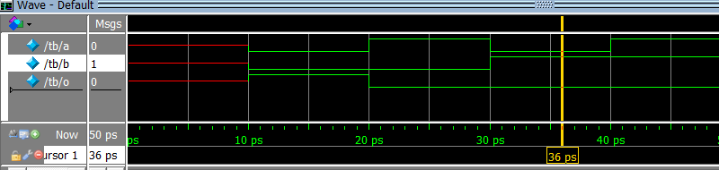 c)
c)
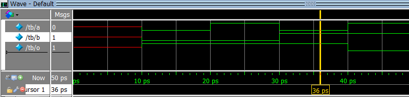 d)
d)
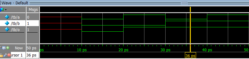 e)
e)
 17.4 What is the result of synthesis of this module?
module design
(
input a,
input b,
input carry_in,
output logic sum,
output logic carry_out
);
logic p, q;
always_comb
begin
p = a ^ b;
q = a & b;
sum = p ^ carry_in;
carry_out = q | (p & carry_in);
end
endmodule
17.4 What is the result of synthesis of this module?
module design
(
input a,
input b,
input carry_in,
output logic sum,
output logic carry_out
);
logic p, q;
always_comb
begin
p = a ^ b;
q = a & b;
sum = p ^ carry_in;
carry_out = q | (p & carry_in);
end
endmodule
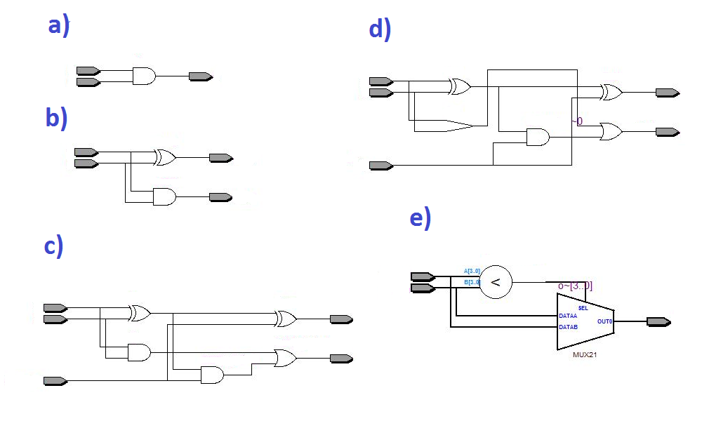 18.4 Which design below corresponds to the schematics on the picture?
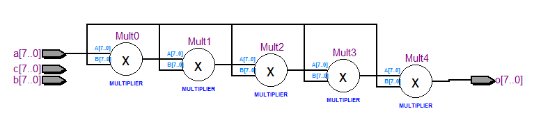 a)
module design
(
input [7:0] a,
input [7:0] b,
output logic [7:0] o
);
always @*
begin
o = a;
if (b < 5)
o = a * a;
end
endmodule
b)
module design
(
input [7:0] a,
input [7:0] b,
input [7:0] c,
output logic [7:0] o
);
always @*
begin
o = a;
for (int i = 0; i < 5; i++)
o *= a;
end
endmodule
c)
module design
(
input [7:0] a,
input [7:0] b,
input [7:0] c,
output logic [7:0] o
);
always @*
begin
int i;
o = a;
for (i = 0; i < 5; i = i + 1)
o = o * a;
end
endmodule
d) both a and c
e) both b and c
19. A designer run FPGA synthesis for the following
4 designs and get the number of logic elements.
However you don't know whether he did it in correct way.
Which set of numbers is more believable for you?
a) 1:16, 2:16, 3:16, 4:16
b) 1:16, 2:16, 3:46, 4:46
c) 1:16, 2:8, 3:46, 4:54
d) 1:46, 2:16, 3:16, 4:46
e) 1:54, 2:45, 3:8, 4:16
module design1 (input [7:0] a, input [7:0] b, input [7:0] c, output logic [7:0] o);
assign o = a + b + c;
endmodule
module design2 (input [7:0] a, input [7:0] b, output logic [7:0] o);
assign o = a + b;
endmodule
module design3 (input [7:0] a, input [7:0] b, output logic [7:0] o);
assign o = a * b;
endmodule
module design4 (input [7:0] a, input [7:0] b, input [7:0] c, output logic [7:0] o);
assign o = a * b + c;
endmodule
20.4 Are there any problems with the following SystemVerilog code?
a) This code is OK
b) Warning: incomplete case statement has no default case item
c) Warning: inferring latch(es) for variable, which holds its previous value in one or more paths through the always construct
d) Warning: variable is read inside the Always Construct but isn't in the Always Construct's Event Control
e) Both (b) and (c)
module design (input [3:0] a, input [3:0] b, input [3:0] c, output logic [3:0] o);
always @(a or b or c)
begin
if (a < b)
o = a + b;
else
o = c;
end
endmodule
21.4 Are there any problems with the following SystemVerilog code?
a) This code is OK
b) Warning: incomplete case statement has no default case item
c) Warning: inferring latch(es) for variable, which holds its previous value in one or more paths through the always construct
d) Warning: variable is read inside the Always Construct but isn't in the Always Construct's Event Control
e) Both (b) and (c)
module design (input [3:0] a, input [3:0] b, input [3:0] c, output logic [3:0] o);
always @*
begin
case (a)
0: o = a + b;
1: o = a - b;
2: o = a * b;
3: o = c;
endcase
end
endmodule
a)
module design
(
input [7:0] a,
input [7:0] b,
output logic [7:0] o
);
always @*
begin
o = a;
if (b < 5)
o = a * a;
end
endmodule
b)
module design
(
input [7:0] a,
input [7:0] b,
input [7:0] c,
output logic [7:0] o
);
always @*
begin
o = a;
for (int i = 0; i < 5; i++)
o *= a;
end
endmodule
c)
module design
(
input [7:0] a,
input [7:0] b,
input [7:0] c,
output logic [7:0] o
);
always @*
begin
int i;
o = a;
for (i = 0; i < 5; i = i + 1)
o = o * a;
end
endmodule
d) both a and c
e) both b and c
19. A designer run FPGA synthesis for the following
4 designs and get the number of logic elements.
However you don't know whether he did it in correct way.
Which set of numbers is more believable for you?
a) 1:16, 2:16, 3:16, 4:16
b) 1:16, 2:16, 3:46, 4:46
c) 1:16, 2:8, 3:46, 4:54
d) 1:46, 2:16, 3:16, 4:46
e) 1:54, 2:45, 3:8, 4:16
module design1 (input [7:0] a, input [7:0] b, input [7:0] c, output logic [7:0] o);
assign o = a + b + c;
endmodule
module design2 (input [7:0] a, input [7:0] b, output logic [7:0] o);
assign o = a + b;
endmodule
module design3 (input [7:0] a, input [7:0] b, output logic [7:0] o);
assign o = a * b;
endmodule
module design4 (input [7:0] a, input [7:0] b, input [7:0] c, output logic [7:0] o);
assign o = a * b + c;
endmodule
20.4 Are there any problems with the following SystemVerilog code?
a) This code is OK
b) Warning: incomplete case statement has no default case item
c) Warning: inferring latch(es) for variable, which holds its previous value in one or more paths through the always construct
d) Warning: variable is read inside the Always Construct but isn't in the Always Construct's Event Control
e) Both (b) and (c)
module design (input [3:0] a, input [3:0] b, input [3:0] c, output logic [3:0] o);
always @(a or b or c)
begin
if (a < b)
o = a + b;
else
o = c;
end
endmodule
21.4 Are there any problems with the following SystemVerilog code?
a) This code is OK
b) Warning: incomplete case statement has no default case item
c) Warning: inferring latch(es) for variable, which holds its previous value in one or more paths through the always construct
d) Warning: variable is read inside the Always Construct but isn't in the Always Construct's Event Control
e) Both (b) and (c)
module design (input [3:0] a, input [3:0] b, input [3:0] c, output logic [3:0] o);
always @*
begin
case (a)
0: o = a + b;
1: o = a - b;
2: o = a * b;
3: o = c;
endcase
end
endmodule