Work in progress: MIPSfpga Lab YP1 Draft 2 to use during the seminars in Almaty, Moscow, Saint Petersburg and Kiev
Этот пост — первый из серии постов, в которых я документирую свой вариант лабораторных занятий с MIPSfpga, который я подготовил в 2015 году и использовал тогда же, в 2015 году на семинарах в Москве (МГУ, МФТИ, МИФИ, МИЭТ), Санкт-Петербурге (ИТМО) и Самаре (СГАУ). Затем я использовал их на семинарах в Санта-Клара, Калифорния и Портленд, Орегон, потом на семинарах в Алма-Ате, и теперь собираюсь использовать на новой серии семинаров в Алма-Ате, Москве, Санкт-Петербурге и Киеве. Кроме этого, часть данных материалов войдет в следущую версию официального пакета MIPSfpga.
Итак:
https://github.com/MIPSfpga/mipsfpga-plus/blob/master/documentation/html_labs/lab_yp1/lab_yp1.html:
MIPSfpga 2.0. Lab YP1. Using MIPSfpga with Serial Loader Flow that does not require BusBlaster board and OpenOCD software
1. Introduction
This lab walks through the alternative usage flow of MIPSfpga, called «Serial Loader Flow». This alternative flow does not require using BusBlaster debugger board and OpenOCD software. While BusBlaster / OpenOCD combination is a flexible and inexpensive way to debug the software uploaded into a synthesized MIPSfpga system, the flow with BusBlaster/OpenOCD has two drawbacks:
- A user is required to buy an additional hardware (BusBlaster) which may not be readily available for some users
- The drivers for OpenOCD depend on third-party software that may not be compatible with some versions of Windows and Linux
The alternative Serial Loader Flow uses USB-to-UART connection already present in Digilent boards with Xilinx Artix-7 FPGA, including Basys3, Nexys4 and Nexys 4 DDR boards. For Altera-based boards that do not have integrated USB-to-UART connections it is still possible to use Serial Loader Flow. This can be accomplished by connecting the board with one of the ubiquitous $5 FTDI-based USB-to-UART connectors readily available in many stores and websites for Arduino hobbyists. Such connectors are easier to get than $50 Bus Blasters available on a smaller number of websites.
In addition to offering the alternative way of uploading software programs into the synthesized MIPSfpga system on FPGA board, this lab illustrates several ideas useful for a digital design student, including:
- The implementation of serial UART protocol
- An example of using a finite state machine (FSM) to parse a text, with FSM coded in Verilog and syntesized in digital hardware rather than parsing the text using an FSM implemented in software
The Serial Loader Flow is also not without drawbacks:
- The Serial Loader Flow does not allow debugging the software on the board using a debugger like Codescape working on a computer,
- Under this flow the hardware has to be aware of virtual-to-physical address mapping. If a user wants to change such mapping, he has to update both software linker script for his programs and Verilog code for the hardware component, specifically the code that translates virtual addresses into physical addresses during uploading the user’s program into a sythesized MIPSfpga system.
Despite those drawbacks, the Serial Loader Flow is a useful option for many users, and it can be used alongside with Bus Blaster / OpenOCD Flow.
2. The theory of operation
2.1. MIPSfpga 2.0 hardware module hierarchy without Serial Loader Flow support
Figure 2.1 shows the basic hierarchy of synthesizable modules of MIPSfpga 2.0 for Digilent Nexys 4 DDR board with Xilinx Artix-7 FPGA and without Serial Loader hardware:

The contents and functionality of each module:
- de0_cv — an external wrapper module, specific for each FPGA board type. The ports of this module correspond to physical ports on FPGA chip itself. The specific module nexys4_ddr is written for Digilent Nexys 4 DDR board with Xilinx Artix-7 FPGA.
- mfp_system — system module, common for all FPGA boards that support MIPSfpga 2.0.
- m14k_top — top-level module of the microprocessor core MIPS microAptiv UP (also referenced in some documentation as MIPS microAptiv MPU). The name m14k is left from the earlier variant of the processor core — MIPS M14Kc.
- mfp_ejtag_reset — a utility module to reset EJTAG debug interface used in Bus Blaster / OpenOCD FlowEJTAG
- mfp_ahb_lite_matrix — a module that combines memory blocks, the controller for AHB-Lite bus and I/O logic. The I/O logic links the addresses coming from the software running on CPU core via AHB-Lite bus, with the signals that control hardware peripherals: buttons, LED indicators etc.
- mfp_ahb_lite_decoder — a module that decode an address on AHB-Lite bus and determines which hardware slave (a memory of an input/output device is going to process the corresponding transaction on the bus
- mfp_ahb_ram_slave reset_ram — an AHB-Lite wrapper for memory blocks. This particular group of memory blocks (reset_ram) is intended for the part of software that starts immediately after the processor exits the reset. This part of software is called «the bootloader».
- mfp_dual_port_ram i0-i3 — modules that infer FPGA block memory during the synthesize. In order for the synthesizer to interpret the code for the module in appropriate way, The code in these modules was written according to special guidelines from EDA (Electronic Design Automation) tool vendors, including Xilinx and Altera, so that the synthesizer interprets the code in appropriate way and infers FPGA-specific block memory. There are four 8-bit wide memory blocks in order to implement 32-bit wide random access memory (RAM). Such design is needed in order to support a single byte-wide AHBLite transfer. The alternative idea with 32-bit wide memory would be not sufficient since neither Xilinx nor Altera support writing 32-bit date in memory with a mask.
- mfp_ahb_ram_slave ram — another AHB-Lite memory wrapper. This group of memory blocks (ram) is intended for the main part of the software program, that is fetched from the cacheable region of the virtual memory map.
- mfp_dual_port_ram i0-i3 — same as above
- mfp_ahb_gpio_slave — AHB-Lite slave implementing GPIO — General Purpose Input / Output. The logic in this module maps bus addresses to the signals used for the peripheral devices: buttons, LED indicators etc.
- mfp_ahb_lite_response_mux — one of submodules used for implementing AHB-Lite bus protocol. Contains a multiplexor that produces correct read data for the CPU based on read data from all memories and I/O slaves. This multiplexor uses the id of a slave stored during the address phase of the corresponding bus transaction in flight
2.2. Serial Loader Flow support in MIPSfpga 2.0 hardware module hierarchy
To support the Serial Loader Flow, for extra modules are added to this structure:

The contents and functionality of the added modules:
- mfp_ahb_lite_matrix_with_loader — this module replaces mfp_ahb_lite_matrix from the previous hierarchy. mfp_ahb_lite_matrix_with_loader contains both mfp_ahb_lite_matrix, as well as three modules with new functionality:
- mfp_uart_receiver — this module receives data from PC through UART and converts this data into a stream of bytes / ASCII characters
- mfp_srec_parser — parses the stream of ASCII characters received from mfp_uart_receiver, interprets these characters as text in Motorola S-Record format, and generates as sequence of transactions (address / data) to fill the memory of a synthesized system with the data described in Motorola S-Record text
- mfp_srec_parser_to_ahb_lite_bridge — converts the transactions, obtained from mfp_srec_parser into transactions that confirm AHB-Lite protocol. This module also converts the virtual addresses used by the software, into physical addresses used by hardware. The conversion is done using simple fixed mapping (nothing complicated like TLB MMU is involved).
Figure 2.3 shows the schematics of mfp_ahb_lite_matrix_with_loader created after Verilog synthesis but before FPGA technology-specific mapping, placement and routing. Note the multiplexor between mfp_srec_parser_to_ahb_lite_bridge and mfp_ahb_lite_matrix. This multiplexor directs to the memory subsystem either the transactions from the CPU core, or the transactions from the Serial Loader:

2.3. More details about module mfp_uart_receiver
mfp_uart_receiver receives data serially from UART RX pin and outputs 8-bit bytes when data is ready. It assumes a simple version of UART protocol, without control signals, and with one start bit. The baud rate and the expected main clock rate is hardcoded. The module contains a state machine that waits for a negative edge (detecting a start bit) and samples data bits by counting clock cycles. Since the width of each symbol is quite big 50,000,000 Hz / 115,200 baud = 434 clock cycles (or 217 for 25 MHz), this method of getting the data is quite reliable:

2.4. More details about module mfp_srec_parser
mfp_srec_parser received data from mfp_uart_receiver and parses them as text in Motorola S-record file format. During parsing the state machine inside mfp_srec_parser forms the transactions to the memory of MIPSfpga+ synthesized system, filling the memory with specified bytes at specified locations. The module header is shown below:

See the description of Motorola S-record format from Wikipedia:

2.5. More details about module mfp_srec_parser_to_ahb_lite_bridge
mfp_srec_parser_to_ahb_lite_bridge is a glue between mfp_srec_parser and AHB-Lite bus. It also edits the addresses, converting virtual addresses into physical according to the rules of fixed mapping (see MIPS microAptiv UP core software documentation):

2.6. Miscellaneous
The output of mfp_srec_parser, a signal called in_progres is used as a reset for microAptiv UP processor core. It means that while the serial loader fills the memory with S-record file data, the processor is not accessing the memory. Once mfp_srec_parser gets the termination record (S7), the core wakes up and starts to fetch the program from the newly filled memory.
The serial loader mechanism does not disable interfacing with regular Bus Blaster / Open OCD. Both ways of loading programs, serial loader and Bus Blaster, can be used without re-synthesizing the system.
3. Setting up the board and connectors
3.1. Setting up Digilent boards with Artix-7 FPGA
The following Digilent boards do no require adding any connectors because they already have USB-to-UART connection embedded in the board:
- Digilent Nexys 4 DDR board with Xilinx Artix-7 FPGA. See the Appendix A about how the board is connected with the applicable peripherals.
- Digilent Nexys 4 board with Xilinx Artix-7 FPGA (no DDR, soon to be discontinued).
- Digilent Basys 3 with Xilinx Artix-7.
Here is an exempt from Digilent documentation about USB-to-UART:

3.2. Setting up Terasic boards with Altera Cyclone II, III, IV and V FPGA
Warning! Make sure to avoid applying voltage to any GPIO pin of FPGA board when the board is not powered. This can damage the pin connection or in severe case FPGA itself.
Some Terasic boards have USB-to-UART connector, for some other boards it is possible to use other interfaces, but for simplicity this lab uses external USB-to-UART connectors attached to general purpose I/O pins.
A picture of FTDI-based USB-to-UART connector with FT232RL chip connected to GPIO pins of Terasic DE0-CV with Altera Cyclone V FPGA. UART TX is connected to the pin 3 from bottom and the ground is connected to pin 6 from the bottom. Note that you need to setup 3.3V/5V jumper on this connector into 3.3V position to avoid potential damage to some sensitive FPGAs:


Serial Loader is also compatible with PL2303TA USB TTL to RS232 Converter Serial Cable module for win XP/VISTA/7/8/8.1. There is another, alternative cable, based on PL2303HX chip however this cable has more compatibility problems with Windows 8.x and we recommend to use cables based on PL2303TA instead:


Same connections can be used with many popular Terasic boards that support MIPSfpga:
- Terasic DE0-CV with Altera Cyclone V
- Terasic DE2-115 with Altera Cyclone IV
- Terasic DE0-Nano board with Altera Cyclone IV FPGA
- Terasic DE0 with Altera Cyclone III
- Terasic DE1 with Altera Cyclone II
See Appendix A for the pictures of all Terasic Cyclone board connections.
4. Running the synthesis and configuring the FPGA with the synthesized MIPSfpga system
4.1. Selecting the appropriate hardware configuration for the lab
Before running synthesis it is necessary to review and possibly modify the file
mfp_ahb_lite_matrix_config.vh
that includes a set of Verilog `define statements that determine the functionality
of the synthesized MIPSfpga system. Make sure that `define MFP_USE_UART_PROGRAM_LOADER
is not commented out:
File mfp_ahb_lite_matrix_config.vh
//
//  Configuration parameters
//

// `define MFP_USE_WORD_MEMORY
// `define MFP_INITIALIZE_MEMORY_FROM_TXT_FILE
// `define MFP_USE_SLOW_CLOCK_AND_CLOCK_MUX
`define MFP_USE_UART_PROGRAM_LOADER
// `define MFP_DEMO_LIGHT_SENSOR
// `define MFP_DEMO_CACHE_MISSES
// `define MFP_DEMO_PIPE_BYPASS
It also may be necessary to configure memory that is built from FPGA block memory cells. By default
the memory for bootloader is 1 KB and the memory for user program is 1 KB. Small block memory fits many older
boards and results in high maximum clock frequency of the synthesized system.
The defines below can be used to increase block memory size. To avoid low max clock frequency
with larger memories and if a lot of memory is necessary, we recommend implementing the interface
to memory chip external to FPGA, such as SDRAM memory present on many FPGA boards.
File mfp_ahb_lite_matrix_config.vh
`define MFP_RESET_RAM_ADDR_WIDTH    10  // The boot sequence is the same for everything

`ifdef SIMULATION
`define MFP_RAM_ADDR_WIDTH          16
`else
`define MFP_RAM_ADDR_WIDTH          10  // DE1: 10, DE0-Nano: 13, DE0-CV or Basys3: 14, Nexys 4 or DE2-115: 16
`endif
4.2. Xilinx Vivado flow
This chapter shows the sequence of steps necessary to synthesize a system based MIPSfpga 2.0
using Xilinx Vivado software and upload it into the board, such as
Digilent Nexys 4 DDR board with Xilinx Artix-7 FPGA on Picture 4.2.1.
Digilent Nexys 4 DDR board with Xilinx Artix-7 FPGA, with optional interfaces and peripherals.
The extra parts are not required for this lab.


After finishing this step the board should be configured with the synthesized design and ready to receive the software.
4.3. Altera Quartus II flow
This chapter shows the sequence of steps necessary to synthesize a system based MIPSfpga 2.0
using Altera Quartus II software and upload it into the board, such as
Terasic DE0-CV with Altera Cyclone V FPGA shown on Picture 4.3.1.
Picture 4.3.1. A picture of
Terasic DE0-CV with Altera Cyclone V FPGA, with interfaces and peripherals.
The extra parts (except FT232RL USB-to-UART) are not required for this lab.

4.3.1. Before installing Altera Quartus II
Note that different Terasic boards and different versions of Windows and Linux require different versions of Quartus II:
- In order to run Altera Quartus II on a computer with 32-bit Windows or 32-Linux,
it is necessary to use Altera Quartus II Web Edition version 13.1
or earlier instead of the later versions. - For older boards (Terasic DE0, DE1, DE2) with Altera Cyclone II/III FPGA, it is necessary to use
Altera Quartus II Web Edition version 13.0 Service Pack 1
or earlier version.
4.3.2. Before running Altera Quartus II
The fastest way to create MIPSfpga project for Quartus II is to use the existing project files located
in board-related directory, such as boards/de0_cv. The contents of such directory include:
The contents of boards/de0_cv directory
de0_cv.qpf
de0_cv.qsf
de0_cv.sdc
de0_cv.v
make_project.bat
make_project.sh
Windows batch file make_project.bat and its Linux equivalent,
Bourne shell script make_project.sh,
create a copy of projects files in a temporary directory named project. The reason for it is:
Quartus II creates a lot of temporary files in the directory where project files are located.
Creating such copy of project files allows to remove those temporary files without removing
project files.
The contents of boards/de0_cv/make_project.bat Windows batch file
rd /s /q project
mkdir project
copy *.qpf project
copy *.qsf project
copy *.sdc project
4.3.3. The sequence of steps


After finishing this step the board should be configured with the synthesized design and ready to receive the software.
5. Compiling the software and uploading it into the synthesized system using Serial Loader
5.1. Files in the first lab directory
| File | Description |
|---|---|
|
00_clean_all.bat |
A set of Windows batch files with self-descriptive names to guide a user through the lab step-by-step. Only 02_compile_and_link.bat, 08_generate_motorola_s_record_file.bat |
|
00_clean_all.sh |
A set of Linux Bourne shell scripts with self-descriptive names to guide a user through the lab step-by-step. Only 02_compile_and_link.sh, 08_generate_motorola_s_record_file.sh |
| boot.S |
Boot sequence, a program in assemply that starts after the processor reset, |
| main.c |
User’s program written in C. |
| makefile |
Makefile that contans basic tasks for compiling and linking the program. |
| mfp_memory_mapped_registers.h |
Header file that contains definitions for the memory-mapped I/O registers |
| modelsim_script.tcl |
A script in Tcl language used by Mentor ModelSim RTL simulator |
| program.ld |
A linker script used by GCC toolchain. |
5.2. The first lab program
The first program just increments the counter and outputs its highest bits
to board-dependent read and green LEDs, as well as the abstracted seven-segment
multiple-digit display peripheral, implemented as a module in top-level board wrapper.
File 01_compile_c_to_assembly.bat
#include "mfp_memory_mapped_registers.h"

int main ()
{
    long long int n = 0;

    for (;;)
    {
        MFP_RED_LEDS   = n >> 16;
        MFP_GREEN_LEDS = n >> 16;
        MFP_7_SEGMENT_HEX = ((n >> 8) & 0xffffff00) | (n & 0xff);

        n ++;
    }

    return 0;
}
Memory-mapped I/O registers are pseudo-variables created using #define
constructs in mfp_memory_mapped_registers.h header file.
The «* (volatile unsigned *)» construct is needed so that the compiler
do not optimize memory accesses to the addresses of memory-mapped I/O registers:
File mfp_memory_mapped_registers.h
#ifndef MFP_MEMORY_MAPPED_REGISTERS_H
#define MFP_MEMORY_MAPPED_REGISTERS_H

#define MFP_RED_LEDS_ADDR       0xBF800000
#define MFP_GREEN_LEDS_ADDR     0xBF800004
#define MFP_SWITCHES_ADDR       0xBF800008
#define MFP_BUTTONS_ADDR        0xBF80000C
#define MFP_7_SEGMENT_HEX_ADDR  0xBF800010

#define MFP_RED_LEDS            (* (volatile unsigned *) MFP_RED_LEDS_ADDR      )
#define MFP_GREEN_LEDS          (* (volatile unsigned *) MFP_GREEN_LEDS_ADDR    )
#define MFP_SWITCHES            (* (volatile unsigned *) MFP_SWITCHES_ADDR      )
#define MFP_BUTTONS             (* (volatile unsigned *) MFP_BUTTONS_ADDR       )
#define MFP_7_SEGMENT_HEX       (* (volatile unsigned *) MFP_7_SEGMENT_HEX_ADDR )

// This define is used in boot.S code

#define BOARD_16_LEDS_ADDR      MFP_RED_LEDS_ADDR

#endif
5.3. First step: cleaning all
This step is optional. It removes all files generated by other steps.
File 00_clean_all.bat
rd /s /q sim

del *.o
del main.s
del program.elf
del program.map
del program.dis
del program*.hex
del program.rec
del FPGA_Ram.elf
5.4. Compiling the software
5.4.1. Compiling C program into assembly to examine the generated code
This step is optional. It can be used to see MIPS assembly code generated by the compiler
for the given C code. When compiling C programs for MIPS platform using GCC toolchain
it is essential to use optimization option, at least -O1. Without optimizations
(-O1) the compiler located all C variable on memory locations rather then
on registers, de facto erasing all the performance advantage of high-performance
RISC core with large register set.
File 01_compile_c_to_assembly.bat
rem -EL           - Little-endian
rem -march=m14kc  - MIPSfpga = MIPS microAptiv UP based on MIPS M14Kc
rem -msoft-float  - should not use floating-point processor instructions
rem -O2           - optimization level
rem -S            - compile to assembly

mips-mti-elf-gcc -EL -march=m14kc -msoft-float -O2 -S main.c
You can compare the code generated with and without optimization below:
The generated main.s MIPS assembly file when compiling with optimization (-O2 option)
main:
	.frame	$sp,0,$31		# vars= 0, regs= 0/0, args= 0, gp= 0
	.mask	0x00000000,0
	.fmask	0x00000000,0
	.set	noreorder
	.set	nomacro
	move	$3,$0
	move	$5,$0
	li	$6,-1082130432			# 0xffffffffbf800000
	li	$11,-256			# 0xffffffffffffff00
	sll	$4,$5,24
.L4:
	srl	$2,$3,8
	or	$2,$4,$2
	sll	$8,$5,16
	srl	$4,$3,16
	andi	$10,$3,0xff
	addiu	$7,$3,1
	and	$2,$2,$11
	or	$4,$8,$4
	sltu	$9,$7,$3
	or	$2,$2,$10
	sw	$4,0($6)
	move	$3,$7
	sw	$4,4($6)
	addu	$5,$9,$5
	sw	$2,16($6)
	b	.L4
	sll	$4,$5,24
The generated main.s MIPS assembly file when compiling without optimization (-O0 option)
main:
	.frame	$fp,16,$31		# vars= 8, regs= 1/0, args= 0, gp= 0
	.mask	0x40000000,-4
	.fmask	0x00000000,0
	.set	noreorder
	.set	nomacro
	addiu	$sp,$sp,-16
	sw	$fp,12($sp)
	move	$fp,$sp
	move	$2,$0
	move	$3,$0
	sw	$2,0($fp)
	sw	$3,4($fp)
.L2:
	li	$2,-1082130432			# 0xffffffffbf800000
	lw	$3,4($fp)
	sll	$3,$3,16
	lw	$10,0($fp)
	srl	$8,$10,16
	or	$8,$3,$8
	lw	$3,4($fp)
	sra	$9,$3,16
	move	$3,$8
	sw	$3,0($2)
	li	$2,-1082130432			# 0xffffffffbf800000
	ori	$2,$2,0x4
	lw	$3,4($fp)
	sll	$3,$3,16
	lw	$10,0($fp)
	srl	$6,$10,16
	or	$6,$3,$6
	lw	$3,4($fp)
	sra	$7,$3,16
	move	$3,$6
	sw	$3,0($2)
	li	$2,-1082130432			# 0xffffffffbf800000
	ori	$2,$2,0x10
	lw	$3,4($fp)
	sll	$3,$3,24
	lw	$10,0($fp)
	srl	$4,$10,8
	or	$4,$3,$4
	lw	$3,4($fp)
	sra	$5,$3,8
	move	$10,$4
	li	$3,-256			# 0xffffffffffffff00
	and	$10,$10,$3
	lw	$3,0($fp)
	andi	$3,$3,0xff
	or	$3,$10,$3
	sw	$3,0($2)
	lw	$10,0($fp)
	lw	$11,4($fp)
	li	$12,1			# 0x1
	move	$13,$0
	addu	$2,$10,$12
	sltu	$14,$2,$10
	addu	$3,$11,$13
	addu	$10,$14,$3
	move	$3,$10
	sw	$2,0($fp)
	sw	$3,4($fp)
	b	.L2
	nop
5.4.2. Compiling C and assembly programs and linking them into ELF file
This step is required. It generates file in ELF format used to define executables for bare metal software
(ELF — Executable and Linkable Format)
File 02_compile_and_link.bat
rem -EL             - Little-endian
rem -march=m14kc    - MIPSfpga = MIPS microAptiv UP based on MIPS M14Kc
rem -msoft-float    - should not use floating-point processor instructions
rem -o program.elf  - output file name
rem -O2             - optimization level
rem -T, -Wl         - linked options

mips-mti-elf-gcc -EL -march=m14kc -msoft-float -O2
    -Wl,-Map=program.map -T program.ld
    -Wl,--defsym,__flash_start=0xbfc00000
    -Wl,--defsym,__flash_app_start=0x80000000
    -Wl,--defsym,__app_start=0x80000000
    -Wl,--defsym,__stack=0x80040000
    -Wl,--defsym,__memory_size=0x1f800
    -Wl,-e,0xbfc00000
    boot.S main.c -o program.elf
5.4.3. Checking program size
This step is optional. This utility outputs the information
that can be used to check if the program fits memory size.
File 03_check_program_size.bat
mips-mti-elf-size program.elf
The output of 03_check_program_size.bat
   text	   data	    bss	    dec	    hex	filename
   1292	     32	     32	   1356	    54c	program.elf
5.4.4. Using disassembly program
This step is optional. It can be used to see the contents of the linked ELF executable.
File 04_disassemble.bat
mips-mti-elf-objdump -D program.elf > program.dis
5.5. Using Verilog simulation to model and debug both hardware and software
This step is optional or can be used as a separate lab.
5.5.1. Preparing Verilog $readmemh file with memory image for the software
This step is optional and is needed only for simulation using Mentor ModelSim,
Icarus Verilog, Xilinx Vivado simulator or any other Verilog simulator.
File 05_generate_verilog_readmemh_file.bat
mips-mti-elf-objcopy program.elf -O verilog program.hex
..\utilities\ad_hoc_program_hex_splitter
MIPSfpga 1.0 package prepared the HEX file to load into ModelSim for simulation using objdump utility
from the standard GCC toolchain, in combination with Windows-only script that was slow. The HEX file in MIPSfpga 2.0
is generated in a different, faster and somewhat more standard way, using objcopy utility from GCC toolchain
with an option «-O verilog», in combination with MIPSfpga 2.0 -specific utility called
ad_hoc_program_hex_splitter.
The utility ad_hoc_program_hex_splitter
splits the file program.hex into two files, program_00000000.hex and program_1fc00000.hex,
that correspond to two physical memory locations — starting from addresses 0x00000000 and 0x1fc00000 correspondingly.
When doing splitting, ad_hoc_program_hex_splitter also converts virtual addresses into byte offsets in the corresponding memories.
In order to load the file created with objcopy and ad_hoc_program_hex_splitter
into 4-byte-wide ram register array, the following testbench code is used in MFP_USE_WORD_MEMORY and non-MFP_USE_WORD_MEMORY modes:


The last step is necessary to load word-wide hex file data into narrow
byte-wide memories necessary for the proper support od byte-wide uncached writes
caused by MIPS instructions SB targeting uncached virtual addresses.
5.5.2. Simulating the system using Mentor Graphics ModelSim
This step is optional. Verilog simulation is the mainstream way of debugging Verilog RTL code.
Mentor ModelSim is a popular low-cost simulator with free version.
This lab is not intended to teach how to use ModelSim, which has a complex GUI
and scripting language to control it by power user. This lab uses a simple Tcl script
that runs the simulation and shows the results on waveforms.
Tcl, or Tool Control Language is a scripting language utilized by many
Electronic Design Automation (EDA) tools.
Windows batch file that invokes ModelSim with Tcl script:
File 06_simulate_with_modelsim.bat
rd /s /q sim
md sim
cd sim

copy ..\*.hex .

vsim -do ../modelsim_script.tcl
The Tcl script used to compile Verilog source code, setup the waveforms and run the sumulation:
File modelsim_script.tcl
vlib work
vlog -vlog01compat +define+SIMULATION +incdir+../../../../../MIPSfpga/rtl_up +incdir+../../.. ../../../../../MIPSfpga/rtl_up/*.v ../../../*.v
vsim work.mfp_testbench
add wave sim:/mfp_testbench/*
run -all
The screenshots outline the steps necessary to observe the results:


5.5.3. Simulating the system using Icarus Verilog
This step is optional.
Verilog simulation is the mainstream way of debugging Verilog RTL code.
Icarus Verilog is the easiest to use Verilog simulator available for the students.
It is free but quite slow, for large designs it is order of magnitude slower
on long runs that expensive commercial simulators like Synopsys VCS and even
commercial version of ModelSim.
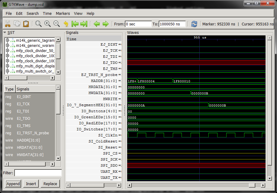
Icarus Verilog is frequently used together with another free tool, GTKWave waveform viever.
The script below compiles Verilog files for MIPSfpga using Icarus Verilog,
runs the simulation and invokes GTKWave viewer with its simple intuitive GUI interface.
File 07_simulate_with_icarus.bat
rd /s /q sim
md sim
cd sim

copy ..\*.hex .

\iverilog\bin\iverilog -D SIMULATION -g2005
    -I ../../..
    -I ../../../../../MIPSfpga/rtl_up
    ../../../../../MIPSfpga/rtl_up/mvp*.v
    ../../../../../MIPSfpga/rtl_up/RAM*.v
    ../../../../../MIPSfpga/rtl_up/*xilinx.v
    ../../../../../MIPSfpga/rtl_up/m14k*.v
    ../../../*.v

\iverilog\bin\vvp a.out > a.lst
\iverilog\gtkwave\bin\gtkwave.exe dump.vcd
during simulation of MIPSfpga using Icarus Verilog simulator
5.6. Uploading software program to the board
5.6.1. Generating the file in Motorola S-Record format
This step is required. Motorola S-Record is a format used by Serial Loader
to load the software into the sythesized MIPSfpga system on FPGA board.
The script uses a standard utility in GCC toolchain called mips-mti-elf-objcopy.
For more information please see Section 2. The theory of operation
File 08_generate_motorola_s_record_file.bat
mips-mti-elf-objcopy program.elf -O srec program.rec
5.6.2. Uploading ELF file into Xilinx FPGA board using BusBlaster and OpenOCD software
This step is optional. Before doing the upload it is necessary to connect BusBlaster to Digilent board as shown on Figure 5.11:

The following script relies on a script for OpenOCD developed for another lab:
File 09_upload_to_xilinx_board_using_bus_blaster.bat
copy program.elf FPGA_Ram.elf
rem Yes, it is working with DE2_115 script
cd C:\MIPSfpga\Codescape\ExamplePrograms\Scripts\DE2_115
loadMIPSfpga.bat C:\github\mipsfpga-plus\programs\00_counter
cd C:\github\mipsfpga-plus\programs\00_counter
del FPGA_Ram.elf
5.6.3. Uploading ELF file into Altera FPGA boards using Bus Blaster and OpenOCD software
This step is optional. Before doing the upload it is necessary to connect BusBlaster to Terasic DE0-CV board as shown on Figures 5.12 and 5.13:


The following script relies on a script for OpenOCD developed for another lab:
File 10_upload_to_altera_board_using_bus_blaster.bat
copy program.elf FPGA_Ram.elf
cd C:\MIPSfpga\Codescape\ExamplePrograms\Scripts\DE2_115
loadMIPSfpga.bat C:\github\mipsfpga-plus\programs\00_counter
cd C:\github\mipsfpga-plus\programs\00_counter
del FPGA_Ram.elf
5.6.4. Checking which virtual COM port is used by USB-to-UART connector
This step is necessary if a user does not know which virtual COM port is used by USB-to-UART connector.
On Windows this information can be obtained from either device manager or from attempting
to run mode command for a number of virtual COM-ports.
File 11_check_which_com_port_is_used.bat
mode com0
mode com1
mode com2
mode com3
mode com4
mode com5
mode com6
mode com7
mode com8
mode com9
pause
mode com10
mode com11
. . . . . . . . .
5.6.5. Finally! Uploading the compiled and linked software program into the synthesized MIPSfpga system on FPGA board via Serial Loader
This step is required.
For Windows the script simply copies the generated Motorola S-record file into the pseudo-file
which corresponds to virtual COM-port used by USB-to-UART connector.
The COM ports existed in Windows from the beginning
and were present even before Microsoft Windows in Microsoft MS-DOS.
Both mode and type commands existed in MS-DOS and later Windows
from the beginning.
Before using this script the user has to modify it by setting the appropriate port number in «a» variable.
The potential problems when using FTDI-based USB-to-UART may be lack of driver
(it can be found on FTDI website) or access control in virtual machine if virtualization is used
(trivial for any admin to resolve).
File 12_upload_to_the_board_using_uart.bat
set a=16
set a=39
mode com%a% baud=115200 parity=n data=8 stop=1 to=off xon=off odsr=off octs=off dtr=off rts=off idsr=off
type program.rec >\\.\COM%a%
For Linux the script is different, but also very simple and uses the standard commands.
The user who runs this script should be included in Linux dialout group
File 12_upload_to_the_board_using_uart.sh
stty -F /dev/ttyUSB0 raw speed 115200 -crtscts cs8 -parenb -cstopb
cat program.rec > /dev/ttyUSB0
After the program is uploaded, the user should be able to see the system working (counting, flashing LEDs).
If it does not work right away, check the port number, the presence of Motorola S-record file, and repeat again.
Appendix A. More pictures for setting up Terasic boards with Altera Cyclone II, III, IV and V FPGA
Some Terasic boards have USB-to-UART connector, for some other boards it is possible to use other interfaces,
but for simplicity this lab uses external USB-to-UART connectors attached to general purpose I/O pins.
Picture A.1. A picture of FTDI-based USB-to-UART connector with
FT232RL chip.
Note that you need to setup 3.3V/5V jumper on this connector into 3.3V position to avoid potential damage to some sensitive FPGAs:

Picture A.2. Serial Loader is also compatible with
PL2303TA USB TTL to RS232 Converter Serial Cable module for win XP/VISTA/7/8/8.1.
There is another, alternative cable, based on PL2303HX chip
however this cable has more compatibility problems with Windows 8.x and we recommend to use cables based on PL2303TA instead:

Picture A.3. A picture of FTDI-based USB-to-UART connector with
FT232RL
chip connected to GPIO pins of Terasic DE0 with Altera Cyclone III FPGA.
UART TX (green) is connected to the pin 3 from right bottom and the ground is connected to pin 6 from right bottom.
Note that you need to setup 3.3V/5V jumper on this connector into 3.3V position to avoid potential damage to some sensitive FPGAs:

Picture A.4. A picture of FTDI-based USB-to-UART connector with
FT232RL
chip connected to GPIO pins of Terasic DE0 with Altera Cyclone III FPGA.
UART TX (green) is connected to the pin 3 from right bottom and the ground is connected to pin 6 from right bottom.
Note that you need to setup 3.3V/5V jumper on this connector into 3.3V position to avoid potential damage to some sensitive FPGAs:

Picture A.5. A picture of
PL2303TA USB TTL to RS232 Converter Serial Cable module for win XP/VISTA/7/8/8.1
connected to GPIO pins of Terasic DE0 with Altera Cyclone III FPGA.
UART TX (green) is connected to the pin 3 from right bottom and the ground (black) is connected to pin 6 from right bottom:

Picture A.6. A picture of
PL2303TA USB TTL to RS232 Converter Serial Cable module for win XP/VISTA/7/8/8.1
connected to GPIO pins of Terasic DE0 with Altera Cyclone III FPGA.
UART TX (green) is connected to the pin 3 from right bottom and the ground (black) is connected to pin 6 from right bottom:

Picture A.7. A picture of FTDI-based USB-to-UART connector with
FT232RL
chip connected to GPIO pins of Terasic DE0-CV with Altera Cyclone V FPGA.
UART TX (green) is connected to the pin 3 from right bottom and the ground is connected to pin 6 from right bottom.
Note that you need to setup 3.3V/5V jumper on this connector into 3.3V position to avoid potential damage to some sensitive FPGAs:

Picture A.8. A picture of FTDI-based USB-to-UART connector with
FT232RL
chip connected to GPIO pins of Terasic DE0-CV with Altera Cyclone V FPGA.
UART TX (green) is connected to the pin 3 from right bottom and the ground is connected to pin 6 from right bottom.
Note that you need to setup 3.3V/5V jumper on this connector into 3.3V position to avoid potential damage to some sensitive FPGAs:

Picture A.9. A picture of FTDI-based USB-to-UART connector with
FT232RL
chip connected to GPIO pins of Terasic DE0-CV with Altera Cyclone V FPGA.
UART TX (green) is connected to the pin 3 from right bottom and the ground is connected to pin 6 from right bottom.
Note that you need to setup 3.3V/5V jumper on this connector into 3.3V position to avoid potential damage to some sensitive FPGAs:

Picture A.10. A picture of
PL2303TA USB TTL to RS232 Converter Serial Cable module for win XP/VISTA/7/8/8.1
connected to GPIO pins of Terasic DE0-CV with Altera Cyclone V FPGA.
UART TX (green) is connected to the pin 3 from right bottom and the ground (black) is connected to pin 6 from right bottom:

Picture A.11. A picture of
PL2303TA USB TTL to RS232 Converter Serial Cable module for win XP/VISTA/7/8/8.1
connected to GPIO pins of Terasic DE0-CV with Altera Cyclone V FPGA.
UART TX (green) is connected to the pin 3 from right bottom and the ground (black) is connected to pin 6 from right bottom:

Picture A.12. A picture of FTDI-based USB-to-UART connector with
FT232RL
chip connected to GPIO pins of Terasic DE0-Nano board with Altera Cyclone IV FPGA.
UART TX (green) is connected to the pin 3 from right top and the ground is connected to pin 6 from right top.
Note that you need to setup 3.3V/5V jumper on this connector into 3.3V position to avoid potential damage to some sensitive FPGAs:

Picture A.13. A picture of FTDI-based USB-to-UART connector with
FT232RL
chip connected to GPIO pins of Terasic DE0-Nano board with Altera Cyclone IV FPGA.
UART TX (green) is connected to the pin 3 from right top and the ground is connected to pin 6 from right top.
Note that you need to setup 3.3V/5V jumper on this connector into 3.3V position to avoid potential damage to some sensitive FPGAs:

Picture A.14. A picture of
PL2303TA USB TTL to RS232 Converter Serial Cable module for win XP/VISTA/7/8/8.1
connected to GPIO pins of Terasic DE0-Nano board with Altera Cyclone IV FPGA.
UART TX (green) is connected to the pin 3 from right top and the ground (black) is connected to pin 6 from right top:

Picture A.15. A picture of
PL2303TA USB TTL to RS232 Converter Serial Cable module for win XP/VISTA/7/8/8.1
connected to GPIO pins of Terasic DE0-Nano board with Altera Cyclone IV FPGA.
UART TX (green) is connected to the pin 3 from right top and the ground (black) is connected to pin 6 from right top:

Picture A.16. A picture of FTDI-based USB-to-UART connector with
FT232RL
chip connected to GPIO pins of Terasic DE1 with Altera Cyclone II FPGA.
UART TX (green) is connected to the pin 3 from right bottom and the ground is connected to pin 6 from right bottom.
Note that you need to setup 3.3V/5V jumper on this connector into 3.3V position to avoid potential damage to some sensitive FPGAs:

Picture A.17. A picture of FTDI-based USB-to-UART connector with
FT232RL
chip connected to GPIO pins of Terasic DE1 with Altera Cyclone II FPGA.
UART TX (green) is connected to the pin 3 from right bottom and the ground is connected to pin 6 from right bottom.
Note that you need to setup 3.3V/5V jumper on this connector into 3.3V position to avoid potential damage to some sensitive FPGAs:

Picture A.18. A picture of
PL2303TA USB TTL to RS232 Converter Serial Cable module for win XP/VISTA/7/8/8.1
connected to GPIO pins of Terasic DE1 with Altera Cyclone II FPGA.
UART TX (green) is connected to the pin 3 from right bottom and the ground (black) is connected to pin 6 from right bottom:

Picture A.19. A picture of
PL2303TA USB TTL to RS232 Converter Serial Cable module for win XP/VISTA/7/8/8.1
connected to GPIO pins of Terasic DE1 with Altera Cyclone II FPGA.
UART TX (green) is connected to the pin 3 from right bottom and the ground (black) is connected to pin 6 from right bottom:

Picture A.20. A picture of FTDI-based USB-to-UART connector with
FT232RL
chip connected to GPIO pins of Terasic DE2-115 with Altera Cyclone IV FPGA.
UART TX (green) is connected to the pin 3 from right bottom and the ground is connected to pin 6 from right bottom.
Note that you need to setup 3.3V/5V jumper on this connector into 3.3V position to avoid potential damage to some sensitive FPGAs:

Picture A.21. A picture of FTDI-based USB-to-UART connector with
FT232RL
chip connected to GPIO pins of Terasic DE2-115 with Altera Cyclone IV FPGA.
UART TX (green) is connected to the pin 3 from right bottom and the ground is connected to pin 6 from right bottom.
Note that you need to setup 3.3V/5V jumper on this connector into 3.3V position to avoid potential damage to some sensitive FPGAs:

Picture A.22. A picture of FTDI-based USB-to-UART connector with
FT232RL
chip connected to GPIO pins of Terasic DE2-115 with Altera Cyclone IV FPGA.
UART TX (green) is connected to the pin 3 from right bottom and the ground is connected to pin 6 from right bottom.
Note that you need to setup 3.3V/5V jumper on this connector into 3.3V position to avoid potential damage to some sensitive FPGAs:

Picture A.23. A picture of FTDI-based USB-to-UART connector with
FT232RL
chip connected to GPIO pins of Terasic DE2-115 with Altera Cyclone IV FPGA.
UART TX (green) is connected to the pin 3 from right bottom and the ground is connected to pin 6 from right bottom.
Note that you need to setup 3.3V/5V jumper on this connector into 3.3V position to avoid potential damage to some sensitive FPGAs:

Picture A.24. A picture of FTDI-based USB-to-UART connector with
FT232RL
chip connected to GPIO pins of Terasic DE2-115 with Altera Cyclone IV FPGA.
UART TX (green) is connected to the pin 3 from right bottom and the ground is connected to pin 6 from right bottom.
Note that you need to setup 3.3V/5V jumper on this connector into 3.3V position to avoid potential damage to some sensitive FPGAs:

Picture A.25. A picture of
PL2303TA USB TTL to RS232 Converter Serial Cable module for win XP/VISTA/7/8/8.1
connected to GPIO pins of Terasic DE2-115 with Altera Cyclone IV FPGA.
UART TX (green) is connected to the pin 3 from right bottom and the ground (black) is connected to pin 6 from right bottom:

Picture A.26. A picture of
PL2303TA USB TTL to RS232 Converter Serial Cable module for win XP/VISTA/7/8/8.1
connected to GPIO pins of Terasic DE2-115 with Altera Cyclone IV FPGA.
UART TX (green) is connected to the pin 3 from right bottom and the ground (black) is connected to pin 6 from right bottom:
